Dye & Pry(Dye stain)은 파괴 Test의 일종으로, PCA의 BGA Solder Crack 및 Solder Joint 관련 불량에 대한 검출 시 사용한다. 인텔에서 작성한 분석가이드로 오래된 자료지만 참고하시길..


Dye & Pry process
Preparation
Equipment/Tools List
–Vacuum Impregnation System
–Custom Vacuum Box (For Board only)
–Tray or paper box for sample transfer
–Beaker
–Dye liquid
Dye
1.Pour the Dye into the beaker till it can fully cover the BGA component, approximate ¾ of the beaker.
2.Place the component vertically or slightly slanted into the beaker to allow dye to flow through the gap.
For the unit mounted on the board.
Use the plasticene to form a wring bar around the chipset unit.
Pour the Dye into the bar
Vacuum
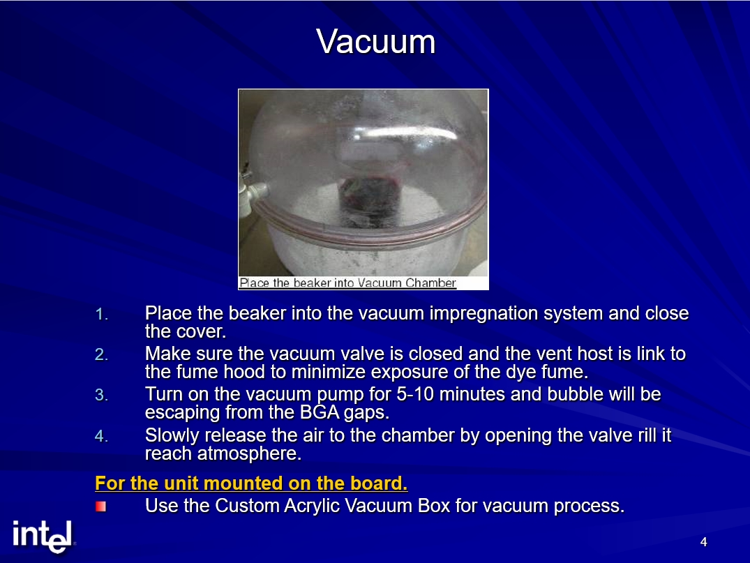
1.Place the beaker into the vacuum impregnation system and close the cover.
2.Make sure the vacuum valve is closed and the vent host is link to the fume hood to minimize exposure of the dye fume.
3.Turn on the vacuum pump for 5-10 minutes and bubble will be escaping from the BGA gaps.
4.Slowly release the air to the chamber by opening the valve rill it reach atmosphere.
For the unit mounted on the board.
Use the Custom Acrylic Vacuum Box for vacuum process.
Cure
1.Remove the component from the beaker by tweezer and let it drip till dry before transfer to a tray.
2.The components were put into a 125C oven for 1 hour in order to cure the dye
3.Pour the remaining dye back into the container for future re-use.
For the unit mounted on the board.
Take out the board from the Custom Acrylic Vacuum Box.
Pour the remaining dye into one beaker for recycle.
Dry & cure the dye as above process
Peel
Peel off the unit from the board with mechanical force.
Peel location was at the middle of the unit’s 4 sides to protect the solder ball at the four corner, which is normally the stress concentrate area and the most likely fail location
The separation area was dyed with red color


